What is a Wafer Frame or Wafer Ring?
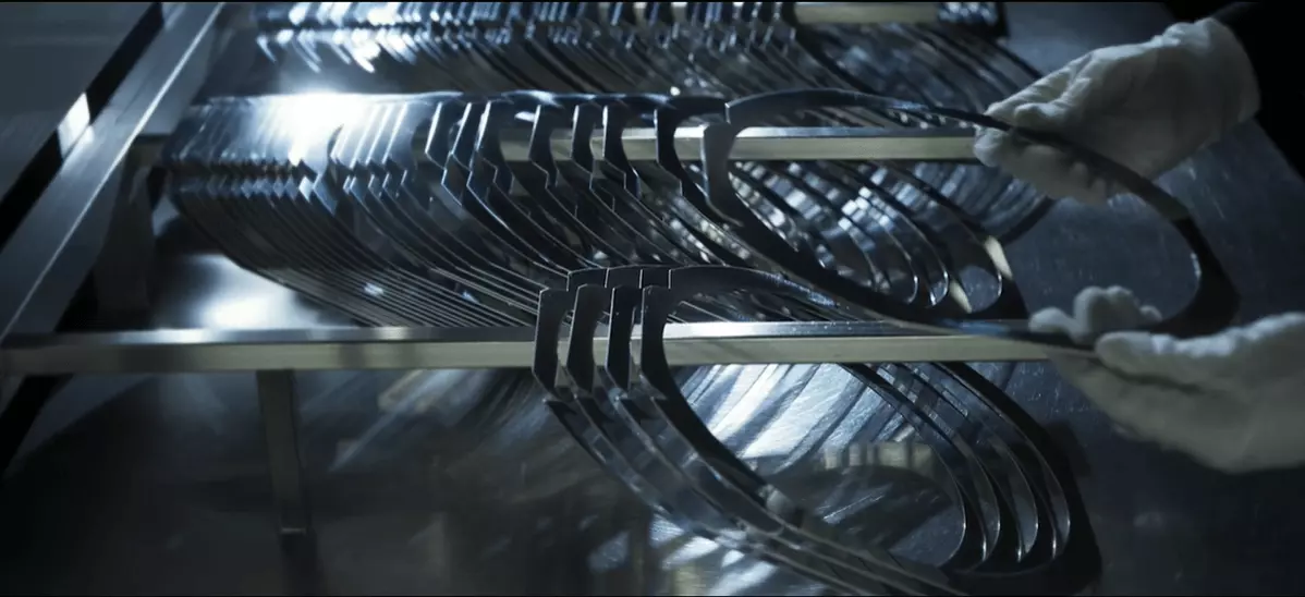
Wafer Frame, also known as Wafer Ring or Dicing Ring, is a stainless-steel frame used in the semiconductor industry to secure wafers during cutting, grinding, and polishing. The frame is typically attached with a protective film to prevent wafers from slipping off during processing. As a reusable product, it can be cleaned and used multiple times without performance degradation.
In semiconductor manufacturing, precision and stability are everything. Each wafer contains thousands of integrated circuits, and even the slightest vibration during cutting can lead to costly defects. That’s why a high-quality wafer frame is indispensable — it provides the rigid, reliable support needed to hold wafers firmly in place throughout complex fabrication steps.
At YJ Stainless, we design wafer frames that meet the highest industry standards. Made from durable 420 stainless steel, our frames are engineered for accuracy, repeatability, and longevity. Whether used in cleanroom conditions or high-volume production, YJ wafer frames maintain exceptional flatness and stability, ensuring flawless wafer handling and superior chip yields.

How a Wafer Frame Is Used
A wafer frame plays a vital role during dicing — the process of cutting a large wafer into individual chips. Here’s how it works:
- Original State – The unused wafer frame is cleaned and inspected.
- Film Attachment – A thin dicing tape is attached to hold the wafer securely.
- Wafer Mounting – The wafer is placed on the film, ready for cutting.
- Processing – The frame keeps the wafer steady as precision blades or lasers cut through it.
This simple but crucial system ensures smooth processing, prevents slippage, and keeps every chip perfectly aligned during production.
Types of Wafer Frames (Wafer Rings/Dicing Rings)
Wafer frames are categorized based on material and application.
1. Plastic Wafer Frames
Lightweight and cost-effective, plastic wafer frames are typically used for:
- General-purpose dicing
- Low-precision processes
- High-volume disposable applications
Pros: Low cost, light weight
Cons: Not reusable, lower rigidity
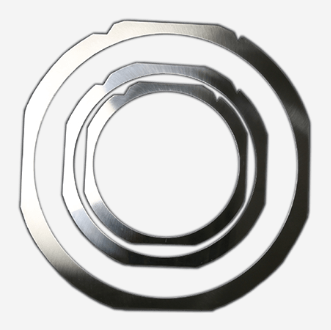
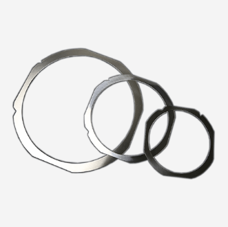
2. Metal Wafer Frames
Made from aluminum or stainless steel, metal frames offer superior rigidity.
Pros:
- High durability
- Excellent flatness
- Suitable for high-speed, high-accuracy dicing
- Ideal for repeated cleaning cycles
Common materials:
- 420 Stainless Steel (industry standard)
- Aluminum alloy
- High-strength steel
Metal wafer frames are widely used in high-end semiconductor packaging lines. In the semiconductor industry, the Japanese DISCO wafer ring, often referred to as a disco frame or disco wafer frame, is recognized as one of the most representative high-precision wafer frames. Many wafer foundries and packaging/testing companies also choose metal frames, plastic frames, or resin frames to accommodate different equipment types and process requirements.
3. Resin Wafer Frames
A hybrid option offering better chemical resistance than plastic and lighter weight than metal.
Pros:
- Chemical-resistant
- Stable structure
- Some models are reusable
Applications:
- Specific chemical-based processes
- Custom or non-standard wafer handling
Why Choose YJ Stainless Wafer Frame/Wafer Ring/Dicing Ring
Customers choose YJ Stainless because we focus on what matters most: price, quality, delivery, and service. With over 40 years of stainless-steel manufacturing experience, we understand how to balance precision and performance, especially in critical components like the dicing ring, at a competitive cost.
YJ Stainless Wafer Frame Specifications:
- Sizes: 6”, 8”, and 12”
- Thickness: 1.2 mm / 1.5 mm
- Material: 420 stainless steel (hot rolled)
- Surface Finish: Bright or matte (customizable)
We also provide professional wafer frame cleaning, laser engraving (barcodes, serial numbers, dates), and custom packaging to match specific production requirements.
Why Clean Wafer Frames?
Cleaning wafer frames is critical because residues, glue, particulates or warpage can lead to:
- mis-alignment during dicing or grinding
- decreased yield due to die damage or chipping
- contamination introduction into the cleanroom environment
By following a proper wafer frame cleaning process, you maintain flatness, remove adhesive/film residues, and ensure the frame is ready for reuse.
How to Clean Wafer Fames?
Our standardized procedure ensures every frame returns to production with original-spec flatness and cleanliness.
1. Inspection & Pre-Processing
- Visual Audit: Detailed check for adhesive buildup, old film, rust, or physical warpage.
- Manual Stripping: Removal of labels, barcode stickers, and heavy tape residue.
- Logging: Data entry of serial numbers to ensure full lifecycle traceability.
2. Debonding & Ultrasonic Cleaning
- Deep Penetration: Frames enter an ultrasonic bath to strip away microscopic glue and particulates from crevices.
- Residue Elimination: Complete removal of dicing-tape films that manual cleaning cannot reach.
3. Rust Removal & Surface Renewal
- Oxidation Treatment: Targeted removal of rust stains using specialized, non-corrosive techniques.
- Surface Buffing: Wiping with specialized dust-free cloths to restore the surface luster and metallic integrity.
4. Grinding, Polishing & Flatness Correction
- Precision Leveling: Automated grinding machines restore surface roughness and correct any mechanical warpage.
- Stability Check: Ensuring the frame meets the rigid flatness requirements for high-speed dicing blades.
5. Laser Engraving & Identification
- Automated Tracking: Application of laser-engraved QR codes, barcodes, or batch IDs.
- Custom Marking: Adding logos or date codes to help your facility manage inventory and rotation cycles.
6. Final Quality Control & Packaging
- Metrology: Final dimensional inspection and flatness verification against spec sheets.
- Cleanroom Prep: Vacuum-sealing in cleanroom-grade bags to prevent contamination during transit.
- Storage: Secure handling to ensure the frame is ready for immediate deployment upon arrival.

Competitive Manufacturing and Reliable Quality
YJ Stainless has spent decades building expertise in stainless steel manufacturing. Our long-term supplier partnerships allow us to secure raw materials at stable, favorable prices — a benefit we pass directly to our customers.
We operate multiple automated production lines that eliminate human error and maintain consistent quality across large-scale production. Every wafer frame is measured, tested, and inspected for flatness, hardness, and dimensional accuracy before leaving our facility.
The result? A high-precision wafer frame that delivers long-term reliability and consistent performance in demanding semiconductor environments.
YJ Stainless Solving Real Customer Challenges
Every customer’s situation is unique, and YJ Stainless takes pride in solving complex wafer frame issues others can’t.
One client reported that frames from another supplier were too slippery, causing wafers to shift during production. After analyzing the problem, YJ introduced a special surface treatment that eliminated slippage completely.
Another customer in Southeast Asia had problems with tape loosening and inconsistent frame sizes. We worked with them through multiple test rounds, refining dimensions and surface finishes until the issue was fully resolved — restoring stability to their production line.
We also listen and adapt. When a customer asked for CPK (Process Capability Index) data, we didn’t hesitate to make it part of our standard quality procedure. That same customer remains a long-term partner to this day.
The Risks of Second-Hand Wafer Frames
Some factories attempt to cut costs by reusing or purchasing second-hand wafer frames. While this may seem economical, it often leads to serious problems. Used frames can have scratches, rust, or uneven shapes, which may affect machine alignment and lead to production errors.
We once accepted a collaboration involving refurbished wafer frames, but the supply quickly became unstable, and prices fluctuated unpredictably. To protect our customers and our reputation for quality, YJ no longer undertakes second-hand projects. Stable quality and consistent supply are simply too important to compromise.
Trusted by Global Semiconductor Leaders
YJ Stainless is proud to be a trusted supplier to some of the world’s top semiconductor companies, including AMKOR, ASE, SONY, TSMC, SanDisk, SPIL, and Micron.
Our manufacturing base in Taoyuan, Taiwan, sits at the heart of Asia’s semiconductor hub, a region known for its advanced technology and strong manufacturing infrastructure. This strategic location allows us to deliver both high performance and fast global service to customers around the world.
Partner with YJ Stainless
If you’re looking for a wafer frame manufacturer that values quality, reliability, and long-term partnership, YJ Stainless is ready to work with you. We combine technical precision with a customer-first mindset, helping semiconductor companies worldwide achieve stable, cost-efficient production.
Contact us now!


