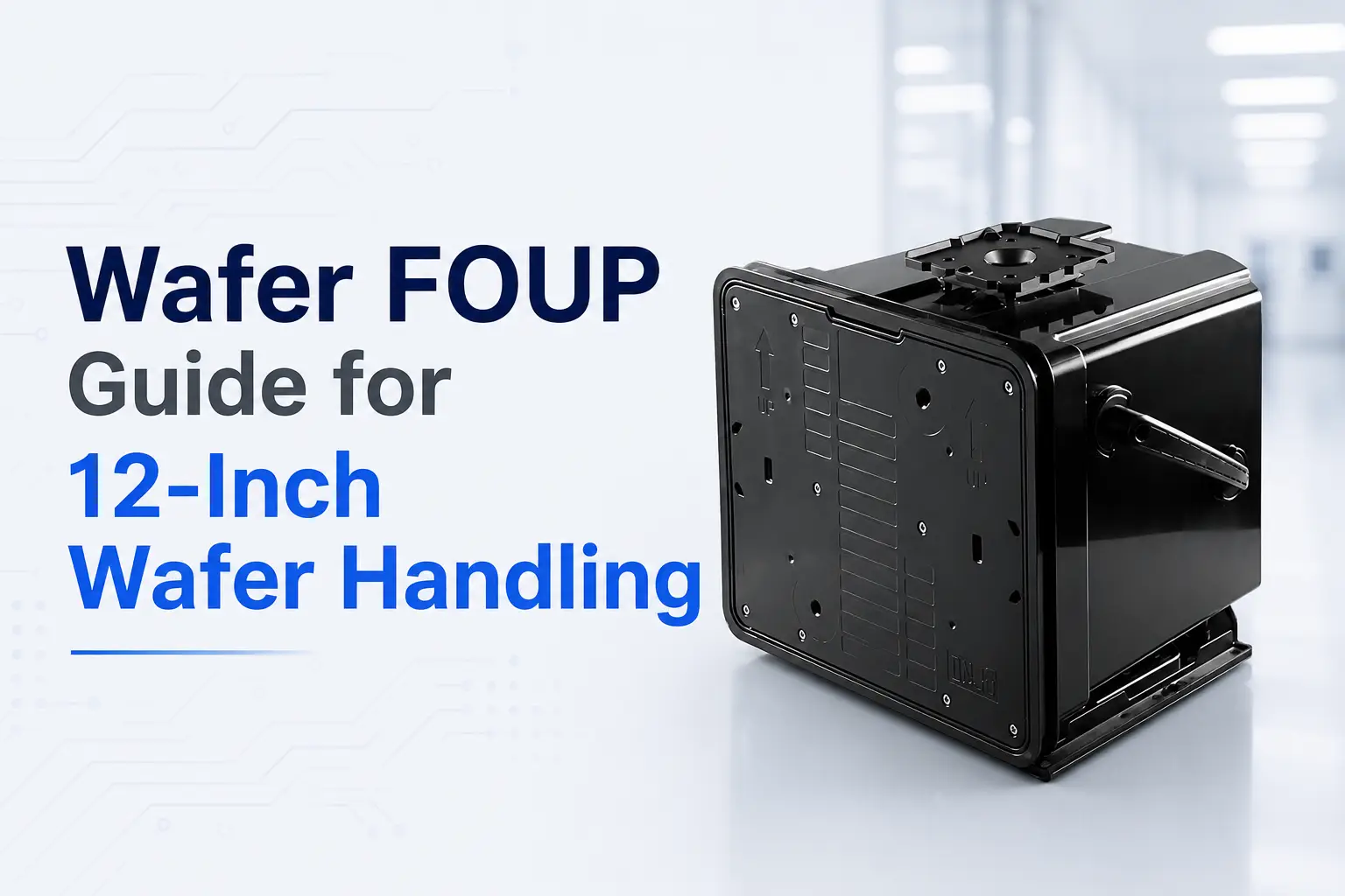
What Is a Wafer FOUP? 12-Inch Wafer Storage, Transport and Cleanroom Handling Guide
A Wafer FOUP, short for Front Opening Unified Pod, is a front-opening wafer carrier used to store and transfer wafers in semiconductor cleanroom environments. It helps protect wafers from particles, electrostatic discharge and unnecessary contact during storage, movement and process handling.
In semiconductor manufacturing, wafers cannot be stored or moved like general parts. They need to stay organized, protected and clean during every transfer step. A Wafer FOUP provides a fixed carrier structure for this purpose, making wafer handling safer and more controlled inside cleanroom production areas.
In simple terms, a Wafer FOUP is not just a box. It is a wafer carrier designed for cleanroom transfer, organized handling and better protection during semiconductor processing.
A Wafer FOUP is usually selected by wafer size, slot capacity, material, ESD protection, front-opening design and equipment interface. For 12-inch wafer handling, it is commonly used for wafer storage, cleanroom transfer and process movement.
What Is a Wafer FOUP Used For in Semiconductor Manufacturing?
A Wafer FOUP is used when wafers need to be stored, transferred or temporarily held with less exposure to the surrounding environment. In semiconductor production, even small particles, static discharge or handling contact can create process risks.
In practice, a FOUP gives wafers a fixed and protected space during transfer, so operators do not need to expose or handle wafers more than necessary.
Common Wafer FOUP applications include:
- 12-inch wafer storage
Keeps wafers organized during temporary storage or process waiting time. - Cleanroom wafer transfer
Supports wafer movement between cleanroom areas, process tools or inspection stations. - Semiconductor wafer handling
Reduces direct handling and helps protect wafers during production workflows. - ESD-safe wafer transport
When made with ESD-safe material, a FOUP helps reduce static-related handling risks. - Process support and temporary holding
Helps keep wafers organized between manufacturing, inspection or transfer steps.
For semiconductor manufacturers, a Wafer FOUP is part of the wafer handling and cleanroom logistics system, not just a storage container.
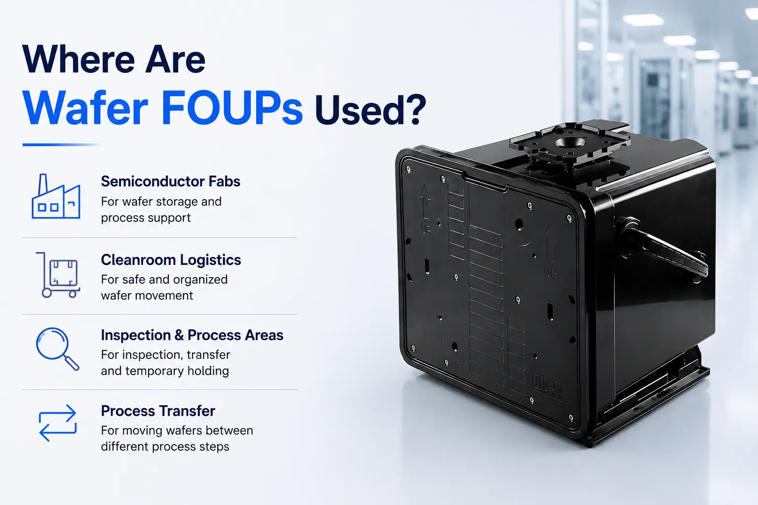
Where Are Wafer FOUPs Used?
Wafer FOUPs are commonly used in semiconductor fabs, cleanroom logistics, wafer inspection areas, process transfer steps and temporary wafer holding. They are especially useful when wafers need to move between different process areas while reducing direct handling and environmental exposure.
For 12-inch wafer handling, a FOUP can help keep wafers organized during storage, movement and production support. The final carrier design should still be confirmed based on wafer size, slot capacity, equipment interface and cleanroom handling requirements.
Wafer FOUP vs Wafer Storage Box
A common misunderstanding is that every wafer box can be used like a FOUP. In practice, a Wafer FOUP is selected when wafer handling involves cleanroom transfer, process movement or equipment-side handling requirements.
A Wafer FOUP and a wafer storage box may both protect wafers, but they are not always used for the same purpose.
A wafer storage box is often used for basic wafer protection. A Wafer FOUP is more focused on cleanroom handling, organized transfer and process-related wafer movement.
Key Factors When Choosing a Wafer FOUP
When selecting a Wafer FOUP, the product name alone is not enough. The carrier must match the wafer size, handling method, cleanroom requirement and process flow.
1. Wafer Size
Confirm whether the carrier is designed for 12-inch wafers, 8-inch wafers or another wafer size. For 12-inch wafer handling, the carrier must support the correct wafer or frame dimensions.
2. Slot Capacity
Slot capacity affects how many wafers or related components can be stored in one carrier. A 25-slot Wafer FOUP is often used when organized multi-slot wafer handling is required.
3. Material
Material affects durability, cleanliness and ESD protection. For semiconductor use, PC ESD material is commonly selected to help reduce electrostatic discharge risks during handling.
4. Front-Opening Design
A front-opening structure allows easier access during cleanroom handling and process transfer. It also helps reduce unnecessary exposure during wafer movement.
5. ESD Protection
Electrostatic discharge can create handling risks in semiconductor production. If wafers or components are sensitive to static, ESD-safe material should be considered.
6. Cleanroom Compatibility
The carrier should be suitable for the cleanroom conditions and transfer method used in the fab. This includes material suitability, carrier cleanliness and handling stability.
7. Customization Needs
Some processes require special slot design, dimension adjustment, RFID support or equipment interface compatibility. In these cases, a custom Wafer FOUP may be more suitable than a standard carrier.
Selection Note: Match the Carrier to the Process
A Wafer FOUP should be selected by process requirement, not only by product name. If the carrier also needs to support SMIF-style pod or tape frame handling, confirm the wafer size, slot pitch, frame size, equipment interface, material and ESD requirement before ordering.
This is especially important when one carrier needs to support both wafer storage and frame handling, because the internal slot design and handling method may be different.
YJ Stainless 12-Inch Wafer FOUP Solution
For 12-inch wafer handling, YJ Stainless provides the TJF-U12-25S 12-Inch Wafer FOUP. It is made with PC ESD material and designed with a 25-slot capacity for cleanroom wafer storage, transfer and semiconductor handling.
Depending on the process requirement, the carrier may also support SMIF-style pod or tape frame handling applications. Custom slot configuration, dimensions and RFID support are available based on actual wafer handling needs.
This solution is suitable for semiconductor fabs, cleanroom logistics, wafer transport and production support where ESD-safe material, organized storage and stable handling are required.
Conclusion
A Wafer FOUP is an important carrier for semiconductor wafer storage, cleanroom transfer and process handling. It helps protect wafers, reduce direct handling and support cleaner, more organized wafer movement.
When choosing a Wafer FOUP, consider wafer size, slot capacity, material, ESD protection, front-opening design, cleanroom compatibility and process requirements.
If you are looking for a 12-Inch Wafer FOUP or a customized wafer carrier for cleanroom handling, YJ Stainless can support standard and custom solutions for semiconductor wafer handling needs.
Contact us now!
FAQ
1. What does FOUP mean in semiconductor manufacturing?
FOUP stands for Front Opening Unified Pod. It is a front-opening wafer carrier used to protect and transfer wafers in semiconductor cleanroom environments.
2. What is a Wafer FOUP used for?
A Wafer FOUP is used for wafer storage, cleanroom transfer and semiconductor wafer handling. It helps reduce direct handling, contamination exposure and static-related risks.
3. Is a Wafer FOUP only used for 12-inch wafers?
Wafer FOUPs are commonly associated with 12-inch wafer handling, but carrier design should always be confirmed by wafer size, slot capacity, equipment interface and process requirement.
4. What is the difference between a Wafer FOUP and a wafer storage box?
A wafer storage box is usually used for basic wafer protection or storage. A Wafer FOUP is more focused on cleanroom transfer, front-opening access, ESD protection and organized process handling.
5. Can a Wafer FOUP support SMIF-style pod or tape frame applications?
Some FOUP-style carriers may support SMIF-style pod or tape frame applications, depending on the carrier design and process requirement. Before ordering, confirm wafer size, slot pitch, equipment interface and whether the carrier is used for bare wafers, wafer frames or tape frames.